
The Significance of Solder Mask in PCB Assembly and Manufacturing
Solder Mask in PCB Assembly and Manufacturing
When constructing a printed circuit board (PCB), solder mask is a necessary and critical step. It insulates the copper traces, prevents unintended electrical connections (called short circuits), and protects the circuit from environmental factors during fabrication and assembly.
In the past, solder mask was applied through a screen-printing process that used ink and a stencil to apply the material to the PCB’s surface. Today, however, most fabricators use liquid photoimageable solder mask material. This type of material can be applied as a liquid or as a dry film, and it is exposed to ultraviolet light to harden the areas that are not to be soldered. Then, the unexposed areas of the mask are rinsed away.
The resulting pattern is then inspected by automated optical equipment to make sure the layer meets all the specifications of the project, and that it correctly covers the copper areas on the PCB that are intended for soldering. If there are any defects or imperfections, touch-up work is performed at this stage. The PCB is then cleaned, sanded down and polished, and then a silkscreen layer is applied to provide the reference designators, pin-one indicators, polarity markers, part numbers and other essential information needed for the project.
Once the silkscreen is finished, the board can undergo a quality control inspection. Then it is ready to be sent on to a specialized pcb assembly and manufacturing company for further processing. In order to prepare the pcb for assembly, the company will first need to receive a copy of the project’s digital file, along with any notes or special requirements from the designer.
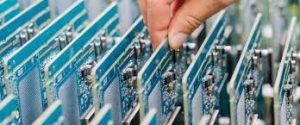
The Significance of Solder Mask in PCB Assembly and Manufacturing
Then the pcb will go through a process called “design for manufacturability” or DFM. This will look at the design specification and ensure that all of the components can be positioned and placed on the board with the correct dimensions, and that they won’t be affected by other factors such as component tolerances or temperature and humidity variations during the assembly process.
After the DFM check is completed, and the pcb is ready for assembly, the company will send the file to its assemblers, who will begin by cleaning the bare pcb to remove any dirt or residues from the silkscreen printing process. Then they will place the parts in their correct positions using a machine that automatically picks and places the components, which is much faster and more accurate than human hand assembly. The pcb will then be inspected visually and connected to a power source to run functional testing and QA tests to ensure that the parts have been positioned correctly and that they are functioning properly. If all of the tests pass, the pcb will be shipped to its final destination.
Flex PCBs, which are designed to be bendable, offer some flexibility, but even they have limitations. Flex PCBs can be bent and folded to a certain degree, which is useful in applications where space is constrained or the board needs to conform to an unusual shape. However, even flexible PCBs are not meant to be crushed or subjected to extreme deformation. They are designed to endure repeated flexing and bending within specified parameters.