
What is the process for creating a prototype custom PCB?
process for creating a prototype custom PCB
PCB prototypes are an essential part of the design and production process. They allow engineers to test their circuit boards and make necessary modifications before the final product is made. Using the right materials, proper soldering, and testing can ensure that your circuit board is functioning as intended.
The first step in creating a custom pcb fabrication is to determine your project requirements. This includes the size, shape, and functionality of the final product. It is also important to select the right PCB layout software. Popular choices include Altium Designer, Eagle PCB, and KiCad. These programs offer a variety of features, from schematic diagrams to layout tools.
Once you have your requirements and design software set up, it is time to begin laying out the circuit board. Start by drafting a schematic diagram, which is a visual representation of the components and their interconnections. Then, position your components strategically to minimize signal interference and maximize performance. Consider factors like trace routing, hole size and placement, and power and ground planes.
Using your PCB layout program, export Gerber files. These are the standard file formats used in electronics manufacturing and contain all of the information needed to fabricate your PCB. Once you have the Gerber files, verify that they meet manufacturing requirements by using a Gerber viewer. This will help you spot any errors that could affect the quality of your prototype.
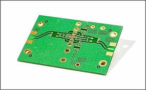
What is the process for creating a prototype custom PCB?
After confirming that your prototype design meets manufacturing requirements, it is time to place an order for fabrication. Choose a manufacturer that offers fast turnaround times, competitive pricing, and high-quality workmanship. PCBGOGOGO offers a wide range of customization options to fit your needs and budget.
Once your PCB is fabricated, it is ready for component assembly. Depending on your design, this may involve using a soldering iron or reflow oven to attach the components. When the PCB is complete, it is important to inspect it for visual defects and any errors in connection traces. If the PCB is a multi-layer board, the individual layers are constructed, with copper foil bonded to each layer to form the conductive traces. Each layer is then etched and drilled according to the design specifications.
Once the board is inspected, it is ready for testing and debugging. This step can identify issues with the components, traces, and connections and prevent them from affecting performance. A thorough debugging process can save valuable time and resources by ensuring that your prototype functions as intended. It can also be beneficial for reducing costs by identifying any potential mistakes that need to be corrected before moving forward with production.
MacroFab offers a full array of testing and inspection services, from in-circuit and functional testing to automated optical inspection (AOI). These services can save you time and money by ensuring that your prototype is error-free before it is sent for production. This allows you to move to the next step in the design and production process with confidence.