
The Effects of Solder Mask on RF PCB Performance
Solder Mask on RF PCB Performance
The solder mask is the primary layer of protection for copper traces on a PCB. It prevents dust and moisture from contacting the copper and hampering its conductivity and integrity. The mask also protects against whiskers, which are thin filaments that grow out of the copper and cause short circuits. It is essential to the overall functionality and reliability of an RF pcb.
There are several factors that impact the quality of solder mask openings, including the material used for the mask, the application process, and curing conditions. The proper choice of these factors can ensure that the solder mask openings on a rf pcb are accurate and consistent, which is essential to improving reliability, performance, and production efficiency.
Solder masks are usually green, red, or brown, and they provide a good contrast against the silkscreen text and components on the PCB for inspection, troubleshooting, and repairs. This contrasting color makes it easy for the operator to distinguish between different areas of the board that require special attention or have been damaged. In addition, the masks help reduce the time spent locating components and their connections, especially in densely packaged layouts.
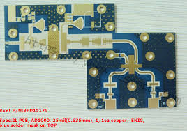
The Effects of Solder Mask on RF PCB Performance
The conductive properties of the copper used in the traces on a RF pcb are highly dependent on the material chosen for the board. The dielectric constant and dissipation factor of the material must be optimum for the intended applications. This is particularly important at high frequencies. The varying distribution of the electrical field within a trace or transmission line caused by the presence of a mask can cause unwanted effects such as reflection and mismatch of impedance.
To avoid these problems, it is necessary to use a high-performance circuit laminate with a low dissipation factor and high dielectric constant for the RF PCBs. It should be able to withstand the changes in temperature and expansion of the traces and pads due to thermal stress. It must also have a low water absorption rate, which is critical in an RF environment.
Besides the material, it is also important to choose a high-quality solder mask that has good adhesion and curing conditions. Moreover, it should be able to withstand environmental conditions, such as humidity. In addition, the mask should be able to withstand thermal and mechanical stress. The manufacturing process must also be streamlined to reduce the risk of delamination, which is the separation or peeling of the solder mask, pads, and copper from the production panel.
The main function of the solder mask is to prevent oxidation and corrosion on the copper traces, which can lead to loss of conductivity and signal interference. However, there are many other functions that it can perform, including preventing shorts between adjacent copper traces and pads, reducing the occurrence of unintended connections during soldering, and providing visual contrast to help identify areas that need special attention. To achieve these goals, the manufacturer must implement advanced equipment and monitoring techniques to ensure that the solder mask has the desired characteristics and quality.