
How to Minimize the Risk of Delamination in Rigid Flex PCBs
Risk of Delamination in Rigid Flex PCBs
Rigid flex PCBs are unique hybrid solutions that merge the best attributes of rigid and flexible circuit boards, delivering an ideal solution for complex electronic applications. They can be utilized in a variety of ways, from foldable wearable devices to aerospace systems and even as conformal heating elements for medical devices. Despite their advantages, rigid flex PCBs are subject to certain challenges that must be addressed.
One of these is the risk of delamination, which can have serious consequences for the integrity and reliability of the circuit board. Delamination can occur due to factors such as material selection, improper fabrication processes, environmental conditions, and more. Effective preventive techniques can minimize the risk of delamination in rigid flex PCBs and ensure they remain functional, reliable, and durable.
rigid flex pcb are subject to a multitude of operational stresses that can impact their structural integrity and overall performance. These include vibration, abrasion, heat, moisture, and other environmental factors. To mitigate the risk of these stresses affecting the rigid flex PCB, designers must carefully evaluate each aspect of the design. This includes examining the stackup, determining pad sizes and locations, and ensuring proper clearances between traces. Additionally, engineers must use appropriate materials and design for mechanical durability to meet the needs of their specific application.
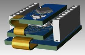
How to Minimize the Risk of Delamination in Rigid Flex PCBs
To mitigate the risks of vibration-induced mechanical stress on a rigid flex PCB, designers should utilize an appropriate material composition. They should also use symmetrical and even material layups and adhere to standard drill-to-copper distances for rigid sections and 7 mil for flex areas. Additionally, designers should avoid splices within the rigid flex area, and utilize a cross-hatched ground plane on the flexible section to increase flexibility.
Another common issue is the lack of an appropriate stiffener in a rigid-flex board, which can lead to flex cracking or failure. This can cause signal degradation, signal skew, and electromagnetic interference (EMI). Engineers can avoid this problem by selecting stiffeners that are specifically designed for rigid-flex boards and using them in the correct locations.
In addition to stiffeners, it is important to utilize a proper pad support and stiffener in a rigid-flex circuit board to reduce stress at those points. Pad supports and stiffeners can help to prevent excessive bending or flexing of the rigid-flex PCB, which is a major cause of delamination. Additionally, pad supports and stiffeners can help to maintain the integrity of conductive traces and minimize stress on their end-faces.
Other important DFM considerations in a rigid-flex PCB include careful characterization of transition zones between the rigid and flexible sections, and compliance with rigid-flex guidelines for bend radius, pad support, and stiffener requirements. Additionally, careful routing and impedance optimization is vital for maintaining signal integrity and EMI control in the flex section of a rigid-flex board.